TPU Trillium v6 has Google's best reported inference numbers and a compelling price-per-FLOP on paper. But the software ecosystem and migration path make the real cost calculation far more complex than a chip-hour comparison suggests. If your stack runs vLLM today, the question is not just "which chip is faster" but "what does it actually cost to move, and does that math ever close."
This post gives you the concrete comparison: architecture, benchmarks where data exists, cost-per-million-tokens, and an honest accounting of what it takes to port a CUDA-based production inference stack to TPU.
What Changed in Trillium v6 (vs v5p)
Trillium is Google's 6th-generation TPU. Google markets two variants: v6e ("edge-efficient," smaller per-chip, lower cost, available in public preview) and v6p ("performance," higher per-chip throughput, more limited availability). This post focuses on v6e since it is the accessible product for most teams.
Memory, Bandwidth, and Systolic Array Design
Each TPU v6e chip carries 32 GB HBM with doubled interchip interconnect (ICI) bandwidth compared to v5p. A four-chip slice aggregates 128 GB across chips; an eight-chip pod reaches 256 GB. The upgraded ICI bandwidth means larger batches can be coordinated across chips without the stalls that limited v5p in multi-chip configurations.
The core compute unit is a matrix multiply unit (MXU), a large systolic array optimized for dense matrix operations. Each chip is effectively one large MXU. This design excels at predictable, regular matrix shapes but is structurally less flexible than GPU streaming multiprocessors for irregular compute patterns. The per-chip BF16 throughput is approximately 918 TFLOPS.
Google reports roughly 30% lower inference cost per token than H100 for large-batch steady-state workloads. Note the comparison: H100, not B200. The B200 generation post-dates those published figures.
Key v6e vs v5p changes:
- ICI bandwidth doubled, reducing multi-chip coordination overhead at large batch sizes
- Memory subsystem upgraded to reduce stalls at batch 32+
- Available per-chip memory unchanged at 32 GB
NVIDIA B200: Where Blackwell Wins on Paper
For full B200 specs and Blackwell architecture details, see the B200 complete guide.
The numbers that matter for this comparison:
| Spec | TPU v6e (per chip) | TPU v6e (4-chip slice) | NVIDIA B200 SXM |
|---|---|---|---|
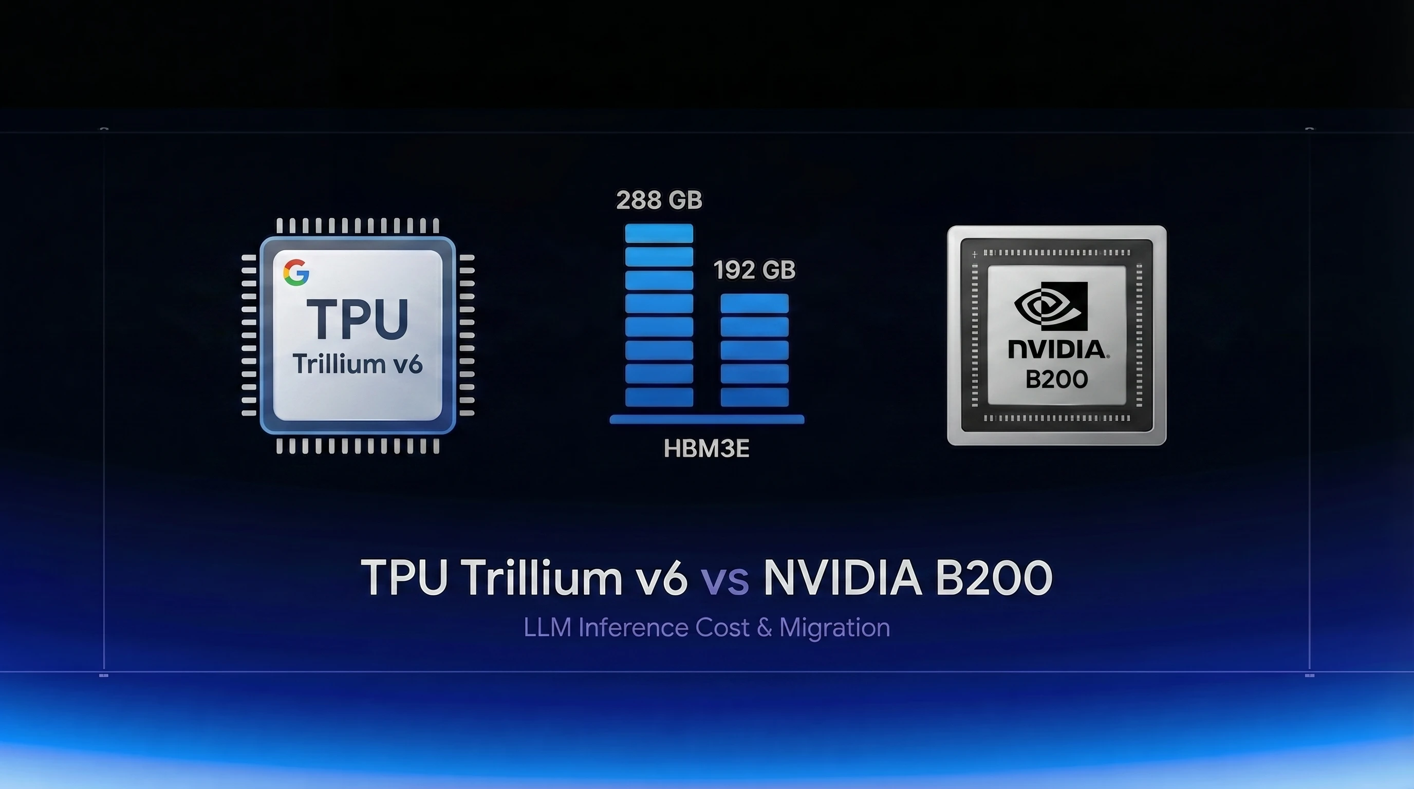
| Memory | 32 GB HBM | 128 GB aggregate | 192 GB HBM3e |
| Memory Bandwidth | ~1.6 TB/s | ~6.4 TB/s aggregate | 8 TB/s |
| Peak BF16 | ~918 TFLOPS | ~3,672 TFLOPS | 2,250 TFLOPS |
| Peak FP8 | Not published | Not published | 4,500 TFLOPS |
| Peak FP4 | Not supported | Not supported | 9,000 TFLOPS |
| Multi-chip interconnect | ICI (doubled vs v5p) | ICI | NVLink 5 (1.8 TB/s) |
| Software stack | JAX, MaxText, Jetstream | JAX, MaxText, Jetstream | CUDA, vLLM, TensorRT-LLM |
The B200 has a per-GPU memory capacity advantage at 192 GB vs 32 GB per chip. Even a four-chip TPU slice (128 GB aggregate) falls short, and multi-chip coordination adds latency. For models above 100B parameters in FP16, the B200 fits more on a single physical unit.
The FP4 gap is significant. Native FP4 Tensor Cores are a B200-specific feature that enables the 9,000 TFLOPS headline throughput for inference. TPU v6e does not support FP4 natively.
Inference Benchmarks: Llama 4 70B and DeepSeek V4 MoE
Direct TPU v6e vs B200 benchmarks on Llama 4 70B are not publicly available as of April 2026. Google's published data uses internal models (Gemma, Gemini variants) at specific batch configs. B200 data comes from MLPerf Inference v6 and public vLLM team benchmarks. Any cross-chip comparison here is an estimate, and the post flags this clearly where relevant.
Tokens Per Second
Google published v6e throughput of approximately 1,000 tokens/sec/chip on Gemma 7B at batch 64 (BF16). For 70B-class models, Google reports 300-400 tokens/sec/chip at batch 8, improving at batch 32+ as the MXU utilization increases.
For B200 on vLLM running Llama 4 70B at BF16, public benchmarks and MLPerf Inference v6 data suggest 800-1,200 tokens/sec per GPU at batch 8. At batch 32+, throughput scales further due to continuous batching and larger KV cache utilization.
| Metric | TPU v6e per chip | B200 per GPU (vLLM) |
|---|---|---|
| Throughput (Llama 4 70B, batch 8) | ~350 tokens/sec (estimated) | ~1,000 tokens/sec |
| Throughput (Gemma/Llama 7B, batch 64) | ~1,000 tokens/sec | ~3,000 tokens/sec (estimated) |
| Time to first token (7B, single user) | 5-20ms (Google reported) | Similar on vLLM + spec decoding |
| p99 latency (batch 32) | Not publicly published | Not publicly published |
These are estimates where noted. Do not use them as production SLA targets without running your own benchmarks on your specific model and serving config.
Time to First Token (TTFT)
Google reports TTFT in the 5-20ms range for v6e at single-user queries on 7B-class models. B200 with vLLM and speculative decoding enabled hits similar ranges for 7B models. At 70B, both chips show higher TTFT, with the exact delta depending on quantization level and serving batch strategy.
p99 Latency at Scale
Neither Google nor major B200 cloud providers have published comparative p99 data for the same model across both platforms. The structural difference is that TPU MXU latency is more predictable (fixed batch shapes, deterministic XLA execution) while GPU/CUDA latency can vary more across irregular request shapes, though modern batching engines handle this well.
For MoE models like DeepSeek V4, TPU's systolic array design is the limiting factor. Expert routing in MoE architectures generates irregular compute patterns that the MXU handles less efficiently than GPU streaming multiprocessors. B200 with vLLM's expert parallelism (EP) mode is a better fit for MoE. For more on MoE inference, see MoE inference optimization on GPU cloud.
Software Ecosystem: The Real Deciding Factor
Hardware specs only matter if the software works. For TPU vs GPU, the software gap is substantial and often underestimated.
JAX, XLA, MaxText, and Jetstream on TPU
TPU workloads run on JAX. PyTorch/XLA provides a bridge, but performance on TPU typically lags native JAX. The production inference stack for TPU looks like:
- MaxText - Google's reference LLM library for JAX, supporting Llama, Gemma, and other open weights
- Jetstream - Google's TPU serving framework with batching and request scheduling
- JAX Pallas - Lower-level kernel programming for TPU, equivalent to writing CUDA kernels but in XLA
Hugging Face transformers has TPU support via accelerate, but model-specific optimizations like paged attention and custom KV cache management are CUDA-only. You get inference, not the optimized inference.
vLLM, SGLang, and TensorRT-LLM on GPU
vLLM, SGLang, and TensorRT-LLM all run natively on CUDA. None of them run on TPU. This is not a feature gap you can close by bumping a config flag. See vLLM vs TensorRT-LLM vs SGLang benchmarks for detailed CUDA framework comparisons.
On the GPU side, you get:
- FlashAttention 3 (CUDA-only, no TPU equivalent with the same maturity)
- AWQ, GPTQ, bitsandbytes quantization (all CUDA-only)
- DCGM-based GPU observability, Prometheus exporters, existing dashboards
- Every open-weight model from Hugging Face, no porting required
Any custom CUDA kernel in your current stack has no TPU equivalent and must be rewritten in XLA or dropped. For running vLLM in production, GPUs are the only realistic option without a major rewrite. For a broader look at the GPU software landscape, see ROCm vs CUDA on GPU cloud in 2026. For a broader look at how Google TPU fits into the hyperscaler ASIC landscape alongside Trainium 3, Maia 200, and Meta MTIA, see Hyperscaler Custom AI Chips in 2026.
Cost Per Million Tokens: What the Numbers Actually Look Like
TPU v6e on Google Cloud
Google Cloud pricing for TPU v6e (on-demand) is approximately $4.20-4.50 per chip-hour, based on publicly available v5e pricing with an estimated 10% uplift for v6e (as of early 2026). You should verify current pricing at cloud.google.com before building a business case, as Google's TPU pricing changes with availability.
For committed use or TPU-specific contracts, discounts apply, but spot-equivalent pricing is not available for TPU in the same way as GPU cloud.
B200 on Spheron GPU Cloud
Live B200 pricing on Spheron: $2.06/GPU/hr spot for B200 SXM6 (4x config, Finland 3, as of 2026-04-19). On-demand pricing is higher; spot pricing is for interruptible workloads.
Cost-per-million-tokens calculation for Llama 4 70B in BF16:
| Metric | TPU v6e (per chip, batch 8) | B200 (per GPU, vLLM, batch 8) |
|---|---|---|
| Chip/GPU cost | ~$4.35/hr | $2.06/hr (spot) |
| Throughput | ~350 tokens/sec | ~1,000 tokens/sec |
| Tokens per hour | 1,260,000 | 3,600,000 |
| Cost per million tokens | ~$3.45 | ~$0.572 |
At batch 64+ (sustained large-batch steady-state), TPU v6e throughput improves substantially, potentially reaching 800-1,000 tokens/sec/chip for 7B models. For large 70B-class models, batch 64 requires coordinating multiple chips, which introduces multi-chip overhead. The cost comparison narrows at very high batch sizes but does not reverse for most production workloads.
For broader cost context, see LLM inference cost economics for 2026.
Pricing fluctuates based on GPU availability. The prices above are based on 19 Apr 2026 and may have changed. Check current GPU pricing → for live rates.
Migration Friction: Porting from CUDA to TPU
Custom CUDA Kernels and torch.compile Graphs
Every custom CUDA kernel in your stack needs an XLA-compatible equivalent or must be dropped. That includes:
- AWQ and GPTQ dequantization kernels (no TPU equivalents, different quantization flow on TPU)
- FlashAttention 3 (CUDA-only; the JAX Pallas equivalent is newer and less battle-tested)
- Any custom attention masks or sparse attention patterns
- CUDA-based KV cache management (paged attention, prefix caching)
torch.compile graphs also need rewrites. XLA tracing has different constraints than torch.compile: shapes must be fixed or handled via XLA's symbolic shape support, and not all PyTorch ops trace cleanly.
FlashAttention and KV Cache Implementations
FlashAttention 3 is a CUDA-only implementation. On TPU, the equivalent is JAX Pallas kernels or the JAX-native attention implementation. The JAX path works but lacks the same depth of optimization and production hardening that FlashAttention 3 has on the CUDA side.
Paged attention (the KV cache optimization that makes vLLM's memory management work efficiently) does not have a direct TPU equivalent. Jetstream has its own batching and KV cache strategy, but the internal implementation differs. Expect to revalidate memory behavior and adjust batch limits after porting.
Realistic Timeline and Effort
For a senior ML engineer porting a production vLLM stack to Jetstream:
- Weeks 1-2: Environment setup, model porting to MaxText/JAX, basic inference validation
- Weeks 3-5: Performance optimization (batching, XLA compilation profiling, memory layout), replacing CUDA-only features
- Weeks 6-8: Serving infrastructure rebuild (Jetstream vs vLLM API surface differences), observability re-integration (Cloud Monitoring instead of DCGM)
- Ongoing: Every new model release or framework update requires separate validation on the TPU path; you cannot assume CUDA updates carry over
Realistic range: 4-12 weeks to reach feature parity and validate quality on evals. The upper end applies if you have extensive custom kernels or non-trivial quantization in the critical path.
The migration cost structure for AWS Trainium 3 is similar, with 2-6 weeks for Neuron SDK porting instead of JAX. See the Neuron SDK migration guide for Trainium 3 for a detailed porting checklist and cost-per-token comparison against H200 and B200 on GPU cloud.
The ongoing maintenance burden is not zero. TPU firmware updates, XLA compiler changes, and MaxText releases are separate from the CUDA ecosystem and require dedicated engineering attention.
When to Pick TPU, When to Pick GPU Cloud
Choose TPU Trillium v6 when:
- You run Google's first-party models (Gemini family) on Google Cloud and are already deeply integrated into the GCP ecosystem
- Workloads are large-batch steady-state inference (batch 32+, continuous throughput), not bursty or variable
- Your stack is JAX-native with no CUDA kernel dependencies
- You are comfortable with single-vendor dependency on Google Cloud (if not, see GPU cloud alternatives to AWS, GCP, and Azure)
Choose GPU cloud (B200 on Spheron) when:
- You use vLLM, SGLang, or TensorRT-LLM in production
- You serve MoE models like DeepSeek V4 where sparse expert routing is in the critical path; see our DeepSeek V4 deployment guide for GPU-specific setup
- You need to run arbitrary open-weight models from Hugging Face without a porting step
- Portability across providers matters; no single-vendor lock-in
- CUDA-dependent custom kernels (AWQ, FlashAttention 3, custom attention masks) are load-bearing
- Your team is CUDA-native and the migration cost would outweigh chip-level savings
For teams running Llama 4 on GPU cloud, see the GPU cloud pricing comparison for 2026 for a full cost breakdown across providers. For GPU hardware comparisons, see the AMD MI350X vs B200 comparison.
Tenstorrent's Wormhole and Blackhole chips take a different approach from both Google TPUs and NVIDIA GPUs. See the Tenstorrent vs NVIDIA hardware comparison for the open-ISA angle.
For a broader view that includes Google's next-generation TPU 8i inference chip (announced at Google Cloud Next 2026), see Google TPU 8i vs NVIDIA Rubin and B200.
Heterogeneous Deployment
For teams at very high scale: a hybrid approach can work. Run large-batch predictable traffic on TPU (document summarization pipelines, batch embedding generation), and handle bursty user-facing inference on GPU cloud. This is operationally complex, two separate serving stacks to maintain, but can optimize cost at sustained high volume if the engineering overhead is justified. Most teams are not at the scale where this trade-off makes sense.
B200 on Spheron matches or beats TPU cost-per-token for most inference workloads once migration and ecosystem overhead are included, with no JAX rewrite required.
B200 SXM6 on Spheron → | View all GPU pricing → | Get started on Spheron →
Frequently Asked Questions
On a raw chip-hour basis, TPU v6e (Trillium) is reported at roughly 30% lower cost than NVIDIA H100, not B200. Compared to B200 on GPU cloud platforms like Spheron (from $2.06/GPU/hr spot), TPU v6e's $4-5/chip-hour on Google Cloud often works out to a higher effective cost once you account for batch size requirements, idle capacity, and the engineering cost of maintaining a JAX/XLA stack.
Not natively. TPU workloads require JAX, PyTorch/XLA, or MaxText. vLLM, SGLang, and TensorRT-LLM are all CUDA-based and do not run on TPUs. Porting a vLLM production stack to TPU requires significant re-engineering using JAX and the MaxText or Jetstream serving frameworks.
TPU v6e is optimized for large-batch, steady-state inference of transformer models. It works best with Google's own models (Gemini family) and with open-weight models ported to JAX via MaxText, including Llama and Gemma variants. Dense models at batch sizes of 32+ are where TPU shows the most advantage. MoE architectures like DeepSeek show more variable performance due to expert routing overhead.
Significant effort is required. Custom CUDA kernels must be rewritten or replaced with XLA-compatible equivalents. torch.compile graphs and any framework-specific optimizations (FlashAttention 3, CUDA graphs) need JAX equivalents. Expect 2-8 weeks of engineering work for a production vLLM stack to reach feature parity on TPU, with ongoing maintenance overhead.
A single TPU v6e chip has 32 GB HBM, which is far less than the B200's 192 GB HBM3e. TPU workloads run across pods of 4 or 8 chips (128-256 GB aggregate), but multi-chip coordination adds latency overhead. For models larger than 100B parameters, the B200's 192 GB per-GPU capacity is a practical advantage.